STRONGLY CORRELATED CONDENSED MATTER PHYSICS
TAKA-HISA ARIMA & YUSUKE TOKUNAGA LAB.
INTRODUCTION OF LABORATORY
We are interested in the strongly-correlated electron systems which show novel physical properties. We design such materials, grow crystals, measure their physical properties, and investigate the origin of the physical responses. Here are some typical examples: / Control of electric polarization of matter with a magnetic field / Change in shape of matter with a magnetic field / Control of magnetism of matter with an electric field / Control of optical property with a magnetic or electric field / Directional birefringence/dichroism / All of these physical responses are related to the simultaneous breaking of symmetries. We often utilize the facilities for synchrotron and neutron experiments to reveal the symmetry breaking.
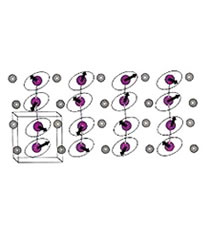
MnWO4гҒ®еј·иӘҳйӣ»зӣёгҒ®гӮ№гғ”гғігҒ®дёҰгҒі
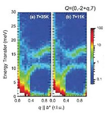
ж”ҫе°„е…үXз·ҡйқһејҫжҖ§ж•Јд№ұжі•гҒ§жё¬е®ҡгҒ—гҒҹгӮүгҒӣгӮ“зЈҒжҖ§еј·иӘҳйӣ»дҪ“гҒ®гғ•гӮ©гғҺгғіеҲҶж•Ј
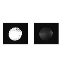
CuB2O4еҚҳзөҗжҷ¶гҒ«гҒӨгҒ„гҒҰиЎЁгҒӢгӮүе…үгӮ’е…ҘгӮҢгҒҹе ҙеҗҲгҒЁиЈҸгҒӢгӮүе…үгӮ’е…ҘгӮҢгҒҹе ҙеҗҲгҒ®йҖҸйҒҺеғҸгҒ®йҒ•гҒ„
MESSAGE
STRONGLY CORRELATED ELECTRON SYSTEMS: FERTILE GROUND FOR DEVELOPMENT OF NEW FUNCTIONAL MATERIALS.
The semiconductor technology is the most significant accomplishment originating from twenty-century solid state physics. The band model well describes the charge carriers in semiconductors, and is very useful for designing many kinds of devices such as diodes, transistors, memories, photodiodes, and CCDs. Nonetheless, the physical properties of all the materials cannot be predicted by the band model. Strong correlation between electrons is a major source of the discrepancy with the band model. A lot of issues related to the strong electron correlation still remain to be solved and hence attract a bunch of researchers. Another reason why we are interested in The strongly correlated electron systems also provide a rich variety of functions. We are exploring novel physical properties arising from strong electron correlation by paying special attention to symmetry breaking.
keyword
Low-temperature physical properties / Magnetism / Strongly correlated electron system / Manganese oxide / X-ray / Coherent imaging / Magnetic structure / X-ray / Imaging / Magnetic phase control / Magnetic imaging / Thermal Hall effect / Anomalous Nernst effect / Anomalous Hall effect / Neutron / X Linear magnetic scattering / resonant X-ray scattering / double perovskite / Raman scattering / synchrotron x-ray / neutron scattering / colossal magnetoresistance / crystal growth / manganite / double perovskite / Raman scattering spectroscopy / synchrotron X-ray / neutron scattering / giant magnetoresistance / Single crystal growth / Electromagneto-optics / Honeycomb structure / Honeycomb lattice / Copper metaborate / Lorentz force of light / Electromagnetic effect / Directional dichroism / Shape memory / Ceramics / Shape memory effect / Strongly correlated systems / Ferroelectric physical properties / Magnetic recording / X-ray absorption edge / Orbital alternation order / Antiferromagnetism / Charge alignment / X-ray magnetic scattering / Charge transfer insulator / Pauli magnetic susceptibility / Optical spectrum / High-pressure synthesis method / Mott transition / Perovskite-type nickel oxide
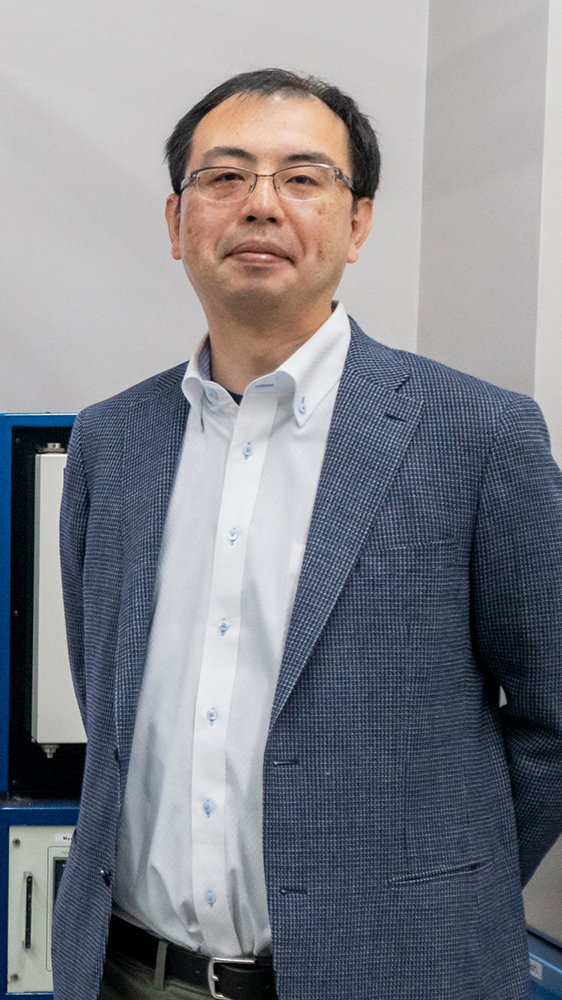
PROFILE : Professor Taka-hisa Arima
1991.9~1995.3: Research Associate, Department of Physics, University of Tokyo
1995.4~1995.10: Research Associate, Department of Applied Physics, University of Tokyo
1995.11~2004.6: Associate Professor, Institute of Materials Science, University of Tsukuba
2004.7~2011.3: Professor, Institute of Multidisciplinary Research for Advanced Materials, Tohoku University
2011.4~present: Professor, Department of Advanced Materials Science, University of Tokyo
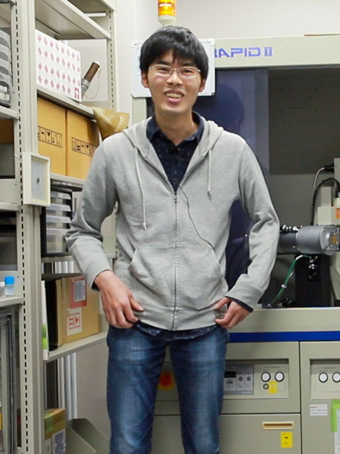
Associate Professor Yusuke Tokunaga
PROFILE
2005.3: Ph. D., Dept. of Applied Physics, University of Tokyo
2005.4~2007.3: Researcher, ERATO Tokura Spin Superstructure Project, JST
2007.4~2011.3: Researcher, ERATO Tokura Multiferroics Project, JST
2011.4~2013.3: ASI Research Scientist, Advansed Science Institute (ASI),RIKEN
2013.4~2014.11: Senior Research Scientist, RIKEN Center for Emergent Matter Science
2014.12~: Associate Professor, Department of Advanced Materials Science, University of Tokyo
keyword
Electromagnetic effect / Cross-correlated physical properties / Multiferroics / Multipole strong order / Chirality / Ferroelasticity / Condensed matter experiments / Strongly correlated electron systems / Magnetic recording / Low power consumption devices / Electric field magnetization control / Multiferroics

STUDENT VOICE : TATSUKI SATO
Prof. Arima and Prof. Tokunaga are cheerful, intelligent, and respectable persons. When the experiment does not go well, they friendly give me advice. They also discuss research directions from a broad perspective, which are very useful for me. In the laboratory, each student energetically carries out research to develop material functions by utilizing the charge, spin, and lattice degrees of freedom. Communication between students are also active. I think that this group provides an environment suitable for those who want to study hard what you like.
APPLIED PHYSICS
Development and experimental research of solid materials exhibiting gigantic response


Taka-Hisa Arima & Yusuke Tokunaga Lab.,
Department Of Advanced Materials Science,
Graduate School of Frontier Sciences,
The University of TokyoKashiwanoha 5-1-5,
Kashiwa,Chiba 277-8561, Japan
+81-4-7136-3805пјҲArimaпјү
arima@k.u-tokyo.ac.jp
+81-4-7136-3770пјҲTokunagaпјү
y-tokunaga@k.u-tokyo.ac.jp
The Goal of Applied Physics
The goal of Applied Physics is to develop a stage = “new material” that can manipulate undeveloped degrees of freedom, to explore unknown phenomena created from that stage and to bring out excellent functions, and to bring out its excellent functions. The purpose is to contribute to the development of human society by elucidating the mechanisms and developing application fields for these phenomena and functions.
AMS (Advanced Materials Science)
Department Office
AMS (Advanced Materials Science),
Graduate School of Frontier Sciences,
The University of Tokyo
Kashiwanoha 5-1-5, Kashiwa, Chiba 277-8561, Japan
Email : ams-office(at)ams.k.u-tokyo.ac.jp
Please change (at) to @.
