
MATERIALS AND OPTICAL SCIENCE
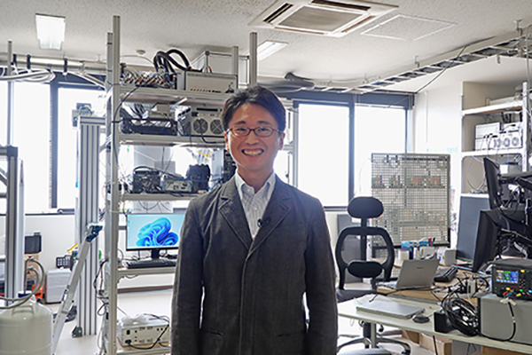
JUN YONEDA LAB.
INTRODUCTION OF LABORATORY
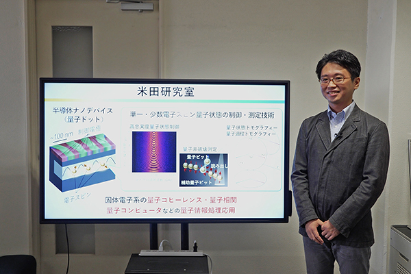
In our laboratory, we focus on experimental research on semiconductor quantum nanodevices to enhance physics understanding of the quantum behaviors of electrons and spins in solid-state devices and to explore their applications in quantum technologies such as quantum computing.
Recent advancements in quantum technology and nanofabrication have enabled us to control and measure the quantum states of single or few electron spins in semiconductor nanodevices (e.g., quantum dots) with high precision and at the single-shot level. By leveraging state-of-the-art technologies for quantum control and measurement of single electrons, we aim to extend the reach of quantum coherence and entanglement in solid-state devices, with critical applications in quantum information processing.
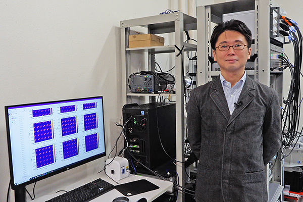
High-fidelity control of the quantum state of a single electron spin
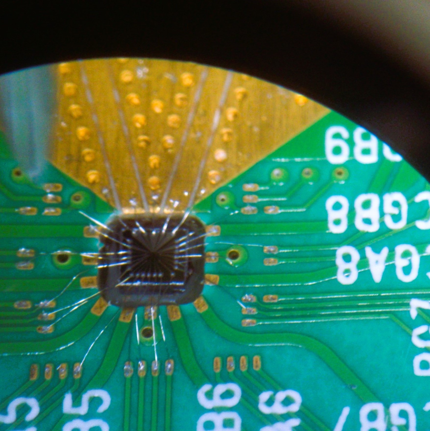
Semiconductor nanodevice chip mounted on a printed circuit board
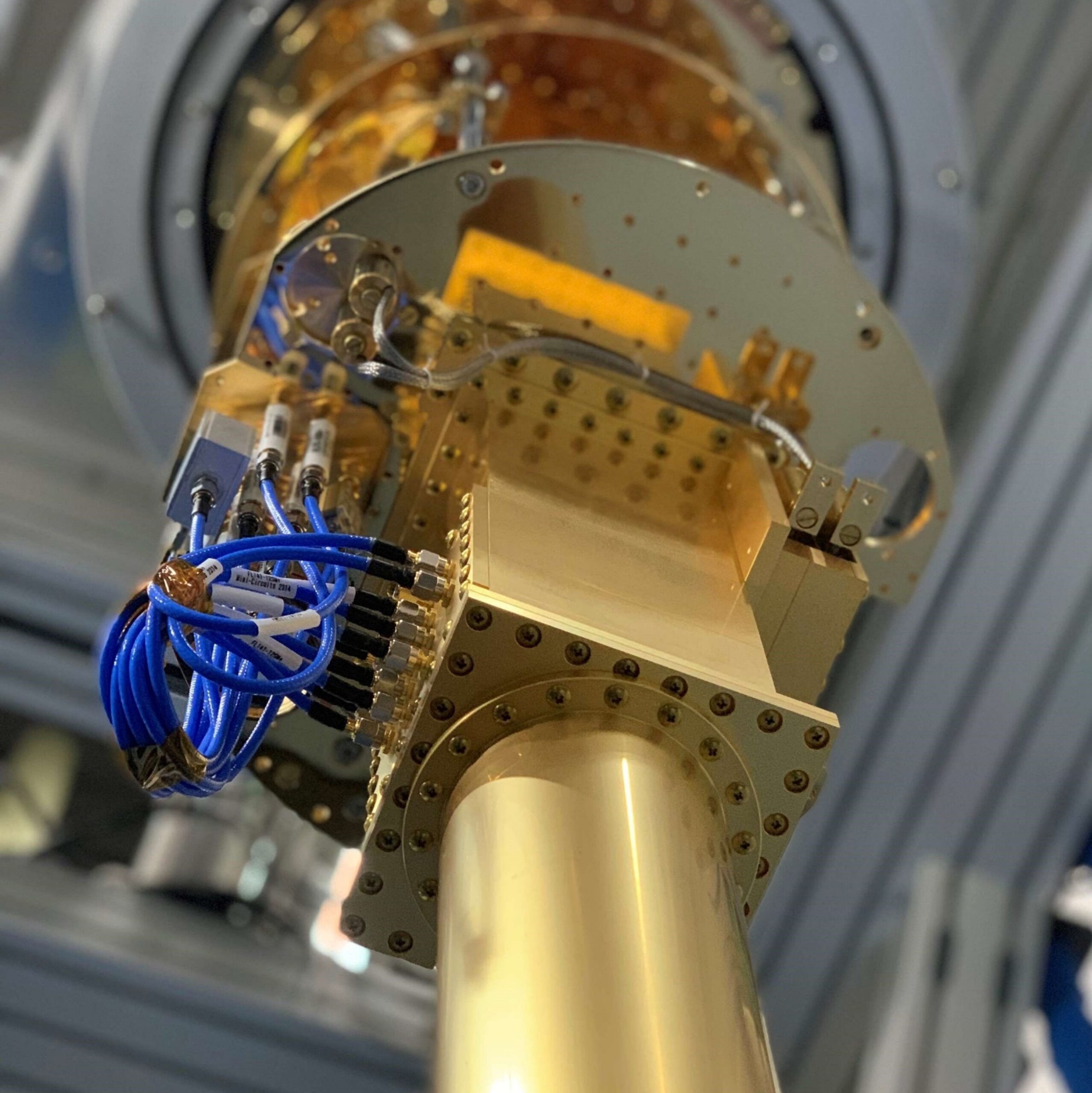
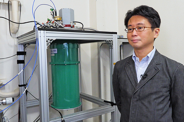
Dilution fridge for quantum device characterization
MESSAGE
Embarking on a Journey to Revolutionize Information Processing with Semiconductor Quantum Technology
From the moment I encountered quantum theory as a freshman, I was captivated by its profound challenge to our conventional understanding of nature. The way counterintuitive theoretical predictions are scientifically tested and verified through sophisticated experiments was nothing short of astonishing. This fascination led me to specialize in quantum technology – a field that harnesses the unique properties of quantum objects for revolutionizing applications such as information processing.
Today, I am deeply involved in research on quantum technology based on semiconductor devices, which are the backbone of our modern information society. This field is rapidly advancing, with numerous groundbreaking demonstrations showcasing its potential.
What excites me most about research is the freedom to explore and develop new ideas. During my graduate studies, I spent countless hours immersed in experiments, driven by passion and curiosity. While achieving the desired results can be challenging, the unparalleled joy of success makes it all worthwhile.
My research endeavors have led me to various universities and institutes inside and outside Japan, and none of these would have been possible without the support of many dedicated colleagues. Finding something you can immerse yourself in is a true blessing, as it definitely contributes to personal growth. I invite you to join us in immersively exploring the frontiers of semiconductor quantum devices and be part of this exciting journey.
Keyword
Semiconductor qubits / Single electrons / Spin manipulation / Quantum devices / Nanodevice physics / Quantum dots / Quantum coherence / Quantum computers / Quantum information processing / Quantum technology
PROFILE : Associate Professor Jun Yoneda
2009 B. Eng., Dept. of Applied Physics, University of Tokyo
2014 PhD (Eng.), Dept. of Applied Physics, University of Tokyo
2014-2015 Postdoctoral Researcher, RIKEN
2015-2018 Special Postdoctoral Researcher, RIKEN
2018-2019 Research Scientist, RIKEN
2019-2020 Postdoctoral Fellow, University of New South Wales
2020-2024 Specially Appointed Associate Professor, Tokyo Institute of Technology
2024 Associate Professor, Department of Advanced Materials Science, University of Tokyo
APPLIED PHYSICS
We aim to control semiconductor devices and apply them to quantum technologies.
Jun Yoneda Lab.
Department Of Advanced Materials Science,
Graduate School of Frontier Sciences,
The University of Tokyo
Kashiwanoha 5-1-5,
Kashiwa,Chiba 277-8561, Japan
+81-4-7136-4133
j.yoneda@edu.ku-tokyo.ac.jp
The Goal of Applied Physic
The goal of Applied Physics is to develop a stage = “new material” that can manipulate undeveloped degrees of freedom, to explore unknown phenomena created from that stage and to bring out excellent functions, and to bring out its excellent functions. The purpose is to contribute to the development of human society by elucidating the mechanisms and developing application fields for these phenomena and functions.
AMS (Advanced Materials Science)
Department Office
AMS (Advanced Materials Science),
Graduate School of Frontier Sciences,
The University of Tokyo
Kashiwanoha 5-1-5, Kashiwa, Chiba 277-8561, Japan
Email : ams-office(at)ams.k.u-tokyo.ac.jp
Please change (at) to @.